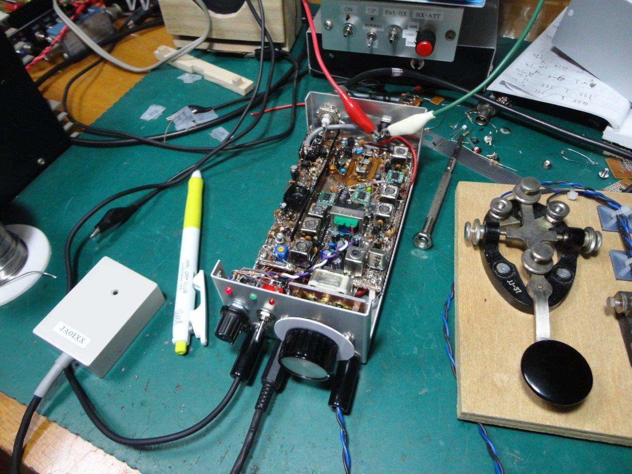
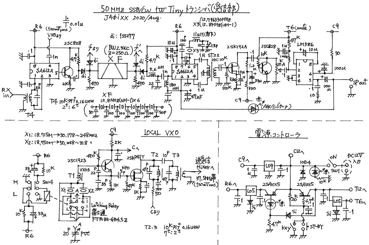
本ギャラリーQRPP-010に展示したトランシーバの受信部は、大変シンプルだが高感度で実用性も高い。消費電流が少ない点は移動用途に好適なので、SA612Aを複数使った同様の構成で、今度はVHFの小型SSB/CWトランシーバを作ることにした。当初の目標イメージは以下の通り。
・箱外形:80×55×150㎜(MB-11)に入れ込む
・重量≦400g (電池除く)
・受信時消費電流≦25mA(無信号時)
・送信出力≧0.5W (0.1Wへ瞬時切換え可)
・周波数:50.180~50.350MHz (IF 12.8MHz)
・受信感度:総合雑音指数(NF) ≦10dB
・電池:単三アルカリ電池×8本(外付け使用)
・省エネ化/小型化のため37.4MHz局発はアナログVXO
・内蔵SPやアナログSメータなどは省略
【VXO】
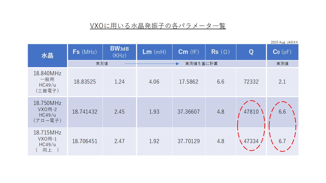
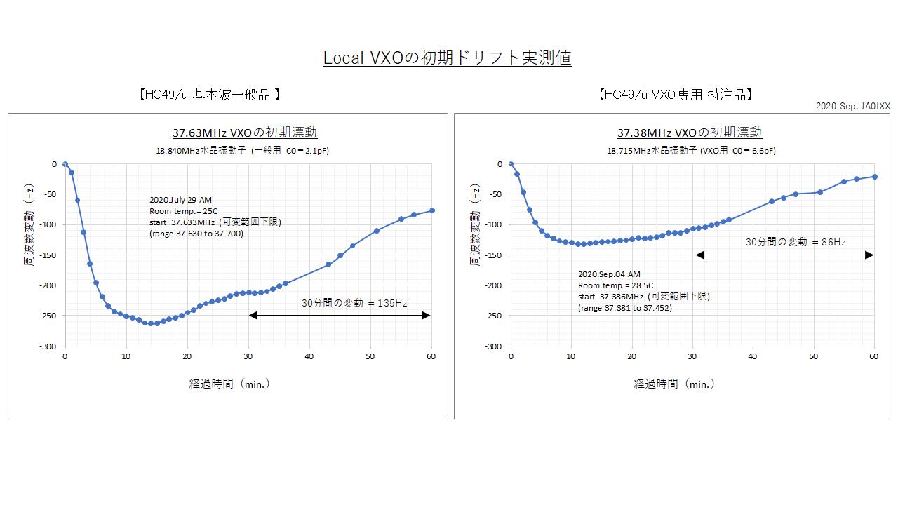
・原振18MHz帯の水晶片は、一般品と特注したVXO専用の二つを比較しながら実験した。VXO用はC0が6.6pFと大きく、Qが小さい点に特徴があり、小さなインダクタンスでも可変域が広くなる(周波数を動かし易い)メリットがある。周波数安定度の向上を期待したが、毎回課題となる下限域での初期ドリフトには顕著な改善は認められなかった。
・実装する二つの水晶切換えには、富士通のラッチングリレーを使用(Others-014参照)した。小型だから実装位置を選ばないし、消費電力は無論ごく僅か。専用駆動回路が無くてもCRだけで動作する。
・局発VXOについてはJG3ADQ永井さんのH/Pが参考になる。参照されたし。
【水晶帯域フィルタ】
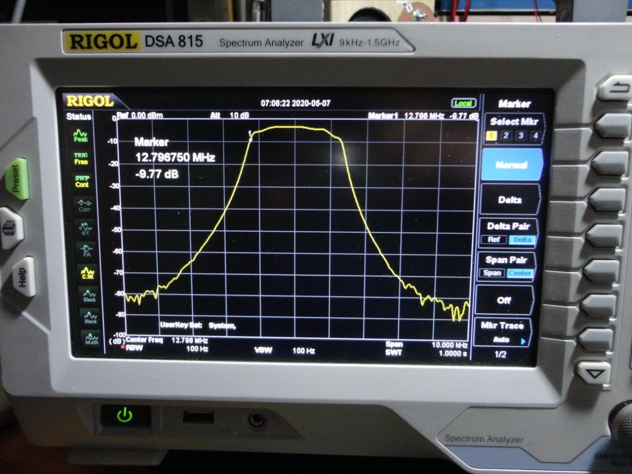
・Measuring equipment-009に展示した、12.8MHz BW 2.4kcのCohn型6素子ラダーフィルタをそのまま使用している。通過特性の良さに加えて、外形サイズの小ささ(わずか10×20mm)が選択の理由。
【BFOの周波数調整】
・一般的なHU49/Uと比べると、C0の小さなUM-1型水晶の発振周波数を動かすのはやや手強い。12.8MHzの発振周波数を3kcほど引き下げるため、最初は10μHのマイクロインダクタを使ったが、温度係数が大きいのか3~4℃の温度変化で周波数が100Hzも動く始末。結局10kコイルボビンのコアに直接0.16㎜UEWを40回ほど巻き、インダクタンス11μHのチョークを自作した。コアの比透磁率は実測2.4、温特もFBで発振周波数は安定している。このコイルQは実測で52だった。
・CWモードでの周波数シフト量は+650Hz。送信時にはセラミックトリマにパラに入れたキャパシタをダイオードで切り離している。
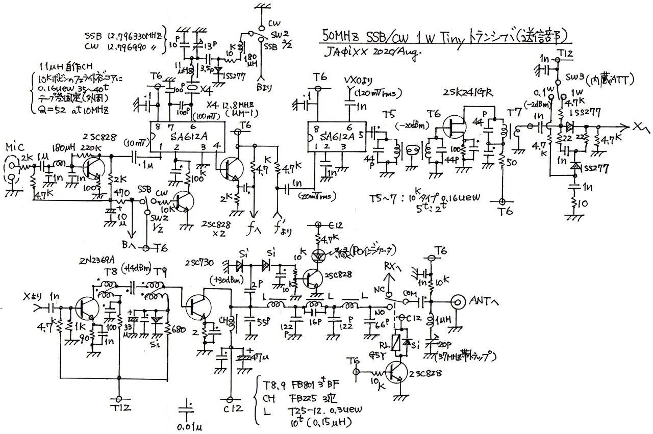
【送信mixer】
・SA612Aは大入力で歪み易いので、入力信号振幅は抑え気味がよい。IMD特性を測ってみたが、最大でもピン端で20mVrms(50Ω系換算で-35dBm)以下が賢明かと思う。
・出力側の負荷を平衡型にすると、シングルエンドの場合より3dB高い出力が取れる。後段の利得マージンが小さい場合には平衡型がベター。
【出力1W⇔0.1W切換え】
・低レベル段にダイオードSW付きATTを置き、SW操作でQRPPに瞬時切換えできるようにしている。リニアアンプ部全体の直線性影響などにより、挿入ATT量を15dBにしてようやく10dBの出力低減を確保した。
【送信スプリアス】
・小さくまとめるため、ドライバーと終段は広帯域回路になっている。その影響で二倍高調波の裸レベルは-10dBと、LC同調方式に比べて15~20dB悪い。パイ型2段LPF装着して実測-37dBなので、最低でも3段フィルタは必須。
【パワーアンプ用素子】
・ドライバーには手持ちの2N2369A(fT700MHz)を使用したが、一般的なトランジスタから選ぶなら2SC2053がFB。アイドル消費電流を抑える観点では終段もバイポーラの方が御し易く、150~300MHzで0.5~1W出せるTO-5(TO-39)型の素子(2SC730,2SC908,2SC1001,2SC1947など)が使えれば最適。
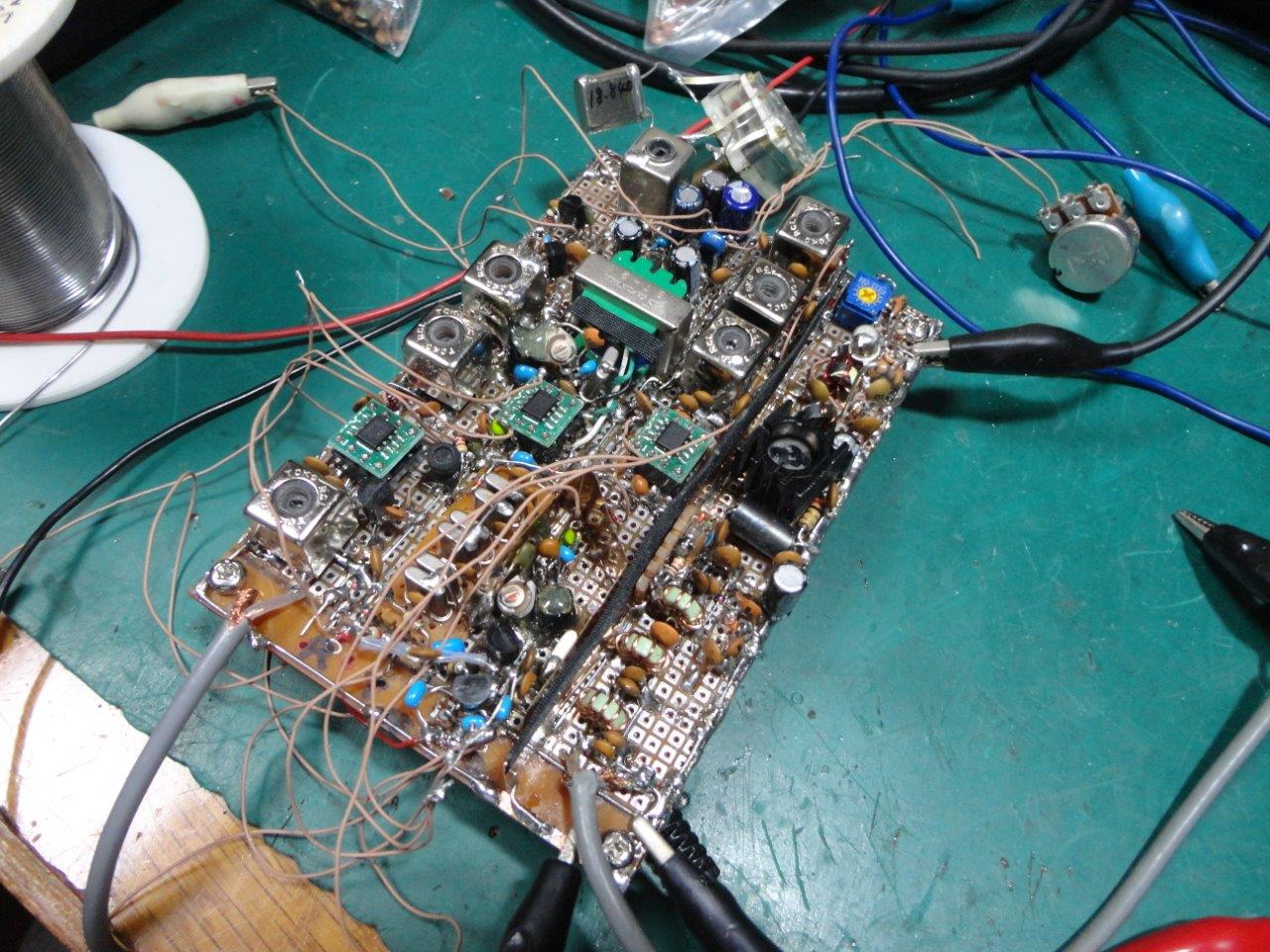
部分テストを重ねながら、73×110mm穴あきボード一枚に部品をギリギリ詰め込みどうやら完成。
次回Part2では、完成後の性能評価結果などについて展示する予定。
The receiver section of the “QRPP-010” transceiver is very simple but sensitive and practical. The point that
consumption current is very little is suitable for portable operation with
battery. So, I planned to manufacture a tiny VHF SSB/CW transceiver for
portable operation using the same “SA612A plus SA612A” style. The specification
considered at first is as follows.
case size 80 x 55 x 150mm, weight≦400g, receiving current≦25mA, output
power≧0.5W, frequency range 50.180~50.350MHz (12.8MHz IF), noise figure≦10dB,
DC12V(UM3 x 8), 18.7 x 2 = 37.4MHz analog VXO for the local OSC, built-in
SP and s-meter are omitted.
【VXO】
I prepared two types of 18MHz crystal which is a half of the needed frequency.
One is usual type, and other one is custom made for exclusive VXO use.
The feature of the latter crystal is big C0 of 6.6pF and small Q. There
is a merit that frequency is easy to vary even if the series inductance
is small. I expected an improvement of frequency stability in the warming-up
period, but conspicuous difference wasn't found at lower end of the frequency
range which shows a drifting problem each time. A latching relay of Fujitsu
was used to change crystal (please refer to Others-014). It’s very small and the power consumption is negligible.
【crystal filter】
A 12.8MHz/2.4kHz minimum Cohn type of crystal ladder filter is being used
(please see measuring equipment-009). The passband shape is good, and the outer size is small enough (only
10 x 20 mm).
【BFO frequency】
It's a little difficult to vary the oscillating frequency of the small
UM-1 of low C0 to be compared with HC49/u. A micro-inductor is not suitable
for the series inductance of crystal because of so big temperature coefficient.
Therefore, I wound 0.16 mm UEW about 40 times on a ferrite screw of 10K
coil bobbin to make an 11μH choke inductance with small temperature coefficient.
Its actual Qu was 52 at 10MHz. BFO frequency is shifted by +650Hz if the
mode is CW. (A small capacitor put on the ceramic trimmer in parallel is
cut off by a diode switch.)
【SA612A mixer】
I measured IMD of SA612A on 50MHz by myself. I think it's better to keep
the input level below 20mV rms (- 35dBm) at most. If an output circuit
of balanced type is chosen, 3dB higher output can be taken out than a single
ended type.
【1W⇔0.1W power reduction】
An ATT with diode SW is put in the low-level stage, and instant change
to QRPP can be done easily. As the linearity of the power amplifier is
imperfect, the inserted ATT was finally set to 15dB to secure 10dB of power
reduction from one watt.
【spurious】
A Non-tuned wide band power amplifier is chosen to make its area small,
thus the naked spurious level of the second harmonics is only -10dBc, which
is 15 to 20dB worse than a LC tuned one. A three stage LPF is a must to
secure the regulation requirement.
【transistors of the RF power stage】
I chose an old but tough 2N2369A for the driver. A TO-5 (TO-39) bipolar
transistor like 2SC730, 2SC908 etc. which can produce 0.5 to 1watt on 150-300MHz
range is preferable for the final from saving space and reducing idling
current point of view.
Doing a partial test, it was finally completed to be packed onto a 73 x
110mm universal board.
It will be exhibited about the result of finished set next time in part 2.