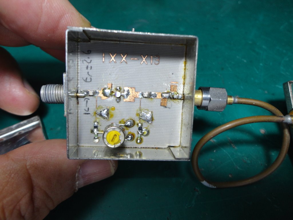
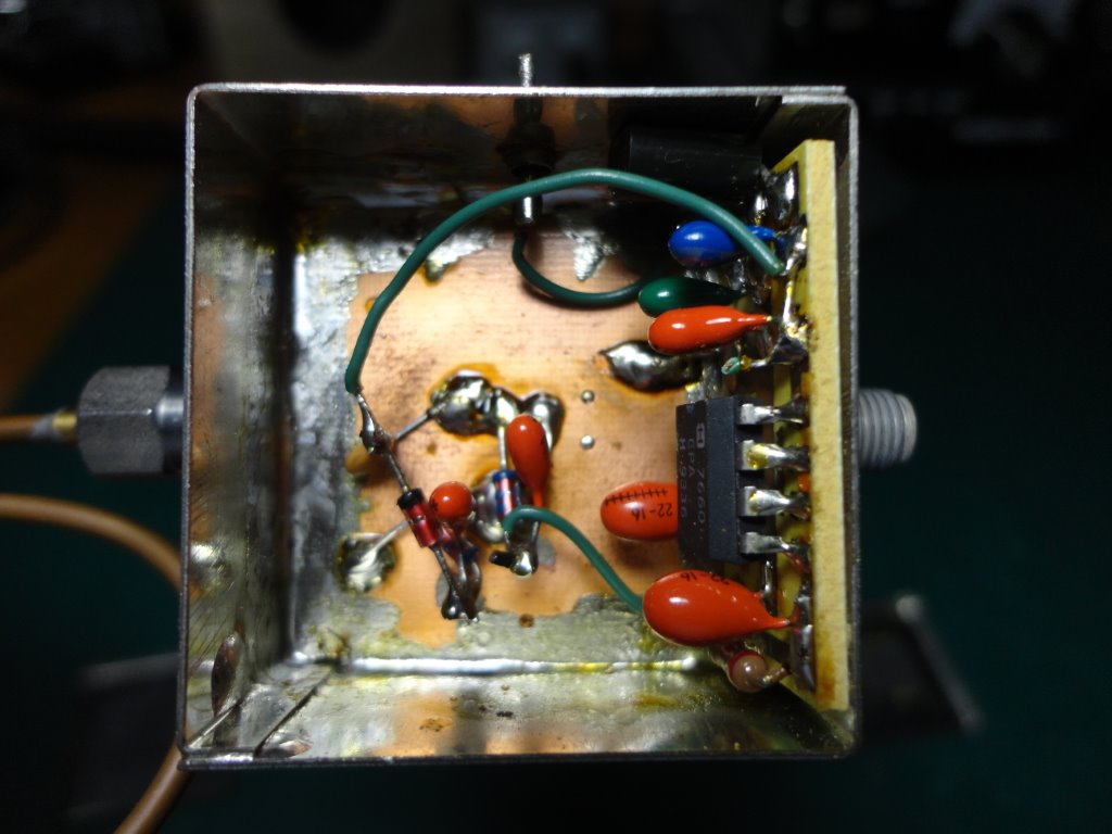
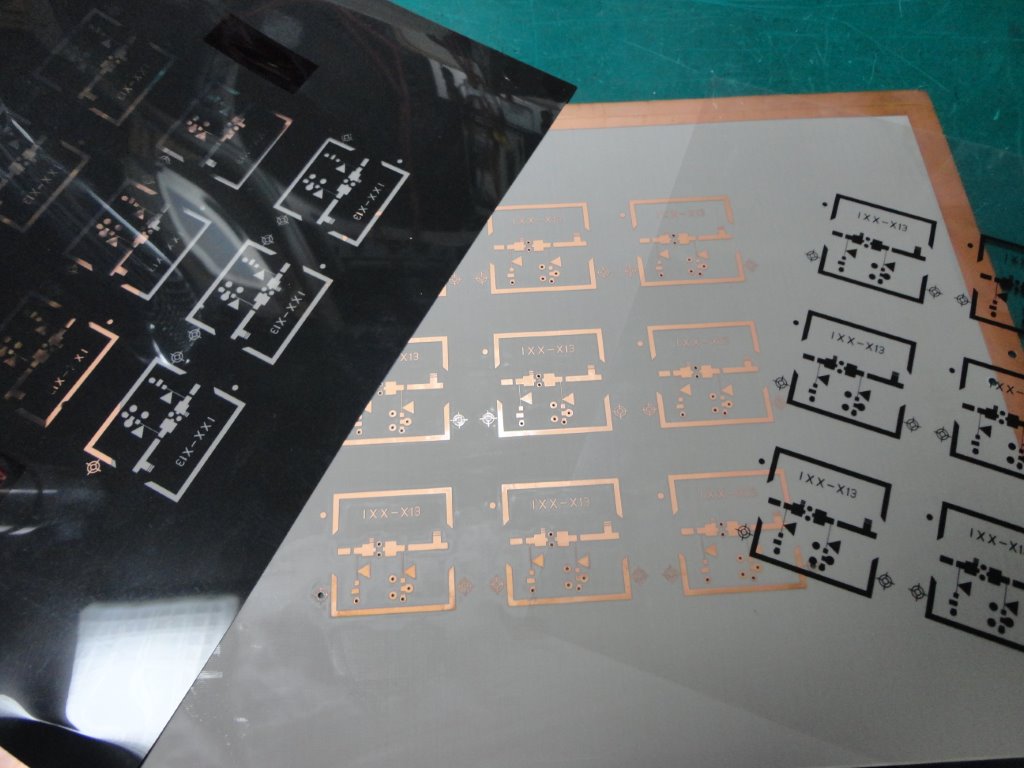
G3WDGが販売していたLNA(WDG-004)を基にして、もっと低雑音なプリアンプを作りたいと思ったのがこれを作るきっかけだった。当時日本では更に性能を高めたHEMTが次々に発表され、中でも富士通のFHX13LGがベストディバイスとの評判になっており、是非それを使おうと決めていた。PCBは0.79mm厚のテフロンガラス基板で、信号ラインのインピーダンス変換パターンはWDGのコピーである。ただオリジナルのWDG-004と違い、ソースのスルーホールを施した上、DCラインの1/4波長チョークスタブも全てプリントパターン化してある。それにより更にローロス化を狙ったつもりだった。この基板はJA0QDE米山さんにお願いしてマスクパターンから作成してもらったが、流石にプロの仕事らしい大変素晴らしい出来映えだった。完成したプリアンプはNF0.85~0.95dB、Gain11.5dBとオリジナル同等の高い性能を示してくれたが、残念ながら目標としていたNF0.7dBはクリアできなかった。ソースパターンやチョークスタブはほぼ最適化されていたと思うが、それでもパターンからの放射ロス等をキャンセルさせるまでには至らなかったということだと思う。1995年のVE3ONTテストでは、このLNAを使って日本で初めて10GHzエコーを捉えることに成功した。なおこの前後にイングランドに住むG3WDGを二回訪ねた。このプリアンプの測定も彼の自宅ベンチで行っている。製作は1994年。
The motive to make this is that I wanted to make more low noise 10GHz preamps
based on LNA (WDG-004) of G3WDG. In those days, HEMT that improved its
performance further was announced one after another in Japan. As the FHX13LG
of Fujitsu was especially famous as the best device for 12GHz, I decided
to use it in the new 10GHz LNA. I chose the Teflon glass substrate of 0.79mm
thickness for the PCB. The impedance conversion pattern of the signal line
is a copy of WDG. However, the source pattern applied the through hole
unlike original WDG-004. Moreover, all 1/4 wavelength chalk stubs of the
DC line are modified to printed pattern, too. I aimed at making to a low
loss further by it. This PCB was manufactured by JA0QDE/Mr. Yoneyama. Because
he was a professional, the make was beautiful indeed. The completed preamp
showed a performance that was the same as the original of NF0.85-0.95dB
and Gain11.5dB. However, NF0.7dB of the target was not able to be cleared
to my regret. I think the source pattern and the chalk stub to have been
optimized almost. Still, it did not come to cancel the radiation loss from
the pattern. In the VE3ONT test in 1995, I succeeded to hear the X-band
moon echo for the first time in Japan using this LNA. I visited G3WDG/Charlie
in England twice around it. This preamplifier was measured at the test
bench in his home shack then. Making was in 1994.